(United Kingdom)

Product Summary
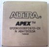
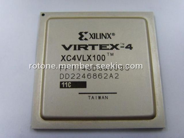
The XC4VLX100-10FF1148 is the newest generation FPGA from Xilinx. The innovative Advanced Silicon Modular Block or ASMBL column-based architecture is unique in the programmable logic industry. XC4VLX100-10FF1148 FPGA contains three families (platforms): LX, FX, and SX. Choice and feature combinations are offered for all complex applications. A wide array of hard-IP core blocks complete the system solution. These cores include the PowerPC processors (with a new APU interface), Tri-Mode Ethernet MACs, 622 Mb/s to 11.1 Gb/s serial transceivers, voltage/temperature system monitor blocks, dedicated DSP slices, high-speed clock management circuitry, and source-synchronous interface blocks. The basic Virtex-4 building blocks are an enhancement of those found in the popular Virtex-based product families: Virtex, Virtex-E, Virtex-II, Virtex-II Pro, and Virtex-II Pro X, allowing upward compatibility of existing designs. XC4VLX100-10FF1148 device is produced on a state-of-the-art 90-nm copper process, using 300 mm (12 inch) wafer technology. Combining a wide variety of flexible features, the Virtex-4 family enhances programmable logic design capabilities and is a powerful alternative to ASIC technology.
Parametrics
XC4VLX100-10FF1148 absolute maximum ratings: (1)VCCINT Internal supply voltage relative to GND: –0.5 to +4.0V; (2)VCCO I/O supply voltage relative to GND: –0.5 to +4.0V; (3)VCCJ JTAG I/O supply voltage relative to GND: –0.5 to +4.0V; (4)VIN Input voltage with respect to GND VCCO < 2.5V: –0.5 to +3.6 V; VCCO ≥ 2.5V: –0.5 to +3.6 V; (5)VTS Voltage applied to High-Z output VCCO < 2.5V: –0.5 to +3.6V; VCCO ≥ 2.5V –0.5 to +5.5V; (6)TSTG Storage temperature (ambient): –65 to +150℃; (7)TJ Junction temperature: +125 +125 ℃.
Features
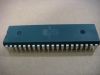
XC4VLX100-10FF1148 features: (1)In-System Programmable PROMs for Configuration of Xilinx FPGAs; (2)Low-Power Advanced CMOS NOR FLASH Process; (3)Endurance of 20,000 Program/Erase Cycles; (4)Operation over Full Industrial Temperature Range(-40℃ to +85℃); (5)IEEE Standard 1149.1/1532 Boundary-Scan (JTAG) Support for Programming, Prototyping, and Testing; (6)JTAG Command Initiation of Standard FPGA Configuration; (7)Cascadable for Storing Longer or Multiple Bitstreams; (8)Dedicated Boundary-Scan (JTAG) I/O Power Supply (VCCJ); (9)I/O Pins Compatible with Voltage Levels Ranging From 1.5V to 3.3V; (10)Design Support Using the Xilinx Alliance ISE and Foundation ISE Series Software Packages.
Diagrams
| Image | Part No | Mfg | Description |  |
Pricing (USD) |
Quantity | ||||||
|---|---|---|---|---|---|---|---|---|---|---|---|---|
 |
 XC4VLX100-10FF1148I |
|
IC FPGA VIRTEX-4LX 1148FFBGA |
Data Sheet |
|
|
||||||
| Image | Part No | Mfg | Description | |
Pricing (USD) |
Quantity | ||||||
|
XC4VFX60-11FFG1152I |
|
IC FPGA VIRTEX-4 FX 60K 1152FBGA |
Data Sheet |
|
|
||||||
|
XC4VFX60-11FFG672C |
|
IC FPGA VIRTEX-4 FX 60K 672-FBGA |
Data Sheet |
|
|
||||||
|
XC4VFX60-11FFG672I |
|
IC FPGA VIRTEX-4 FX 60K 672-FBGA |
Data Sheet |
|
|
||||||
|
XC4VLX100-10FF1148I |
|
IC FPGA VIRTEX-4LX 1148FFBGA |
Data Sheet |
|
|
||||||
|
XC4VLX100-10FF1513I |
|
IC FPGA VIRTEX-4LX 1513FFBGA |
Data Sheet |
|
|
||||||
|
XC4VLX100-10FFG1148C |
|
IC FPGA VIRTEX-4 100K 1148-FBGA |
Data Sheet |
|
|
||||||